This website uses cookies to enable its essential functions, personalize content and advertisements, provide social media features, and analyze website traffic. We may also share information about your use of our site with our social media, advertising, and analytics partners.
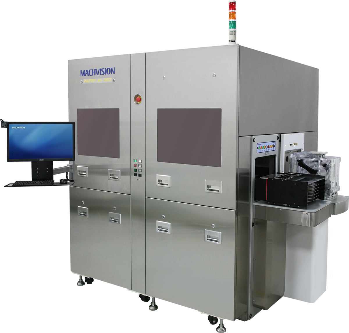
Wafer AVI
Wafer AVI is a high-efficiency inspection system specifically engineered for semiconductor back-end assembly and testing and wafer fabrication processes.
It features deep integration of optical acquisition, advanced image processing algorithms, and AI-driven deep learning technologies. The core objective is to supersede conventional manual visual inspection which is characterized by high labor costs and fatigue-induced errors—thereby providing the industry with a high-quality, cost-effective, and high-throughput fully automated inspection solution.
In terms of technical performance, the system utilizes high-resolution line-scan imaging technology. This allows the system to achieve a precise equilibrium between inspection throughput and metrological accuracy during high-speed scanning. This system is primarily deployed for final visual inspection post-wafer dicing or prior to packaging. It is particularly well-suited for mid-to-late stage inspection in advanced packaging processes such as FOWLP and CoWoS, ensuring that every die adheres to stringent quality standards before proceeding to the next process node.
